半导体材料 Semiconductor materials
6 英寸硅衬底
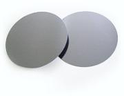
•单面(研磨)镜面抛光
•製法:CZ
•P型
•結晶方位:<111>
•电阻率:1~4 Ωcm
•厚度:675±15μm
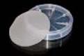
•直径:150mm
|  |
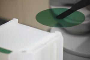
GaN-Single Crystal Substrate
| Orientation: | c-axis (0001) +/- 1.0 o |
| Nominal Thickness: | 250+/- 50 um |
| Dimension: | 50.8mm+/-1mm |
| Bow | <5 microns |
| TTV | <10 microns |
| Conduction Type: | N+ type |
| Resistivity | < 0.05 Ohm-cm |
| Dislocation Density | < 5x106cm-2 |
| Macro Defect Density | < 5 cm-2 |
| Transmission | => 70%
( click here to see transmission curve ) |
| Front Surface Finish: | (Ga Face) , Epi-ready,RMS <1 nm |
| Back surface finish: | N-face Epi-ready,RMS <1 nm |
| Edge Exclusion Area: | 1 mm |
| Package: | Single Wafer Container or membrane box |
|  |
STANDARD SPECIFICATION FOR 100MM DIAMETER ON-AXIS
SEMI-INSULATING SIC SUBSTRATES
| Diameter: | 100.0 +0.0/-0.2 mm |
| Polytype: | 4H |
| Orientation: | {0001} ±0.25 deg |
| Type: | Semi-insulating (HTCVD high purity) |
| Resistivity: | ≥ 1E7 Ohm-cm |
| Thickness: | 500 ± 25 μm |
| TTV: | ≤ 5 μm |
| LTV: | ≤ 2 μm |
| Warp: | ≤ 45 μm |
| MPD (1mm edge exclusion): | ≤ 5 cm-2 |
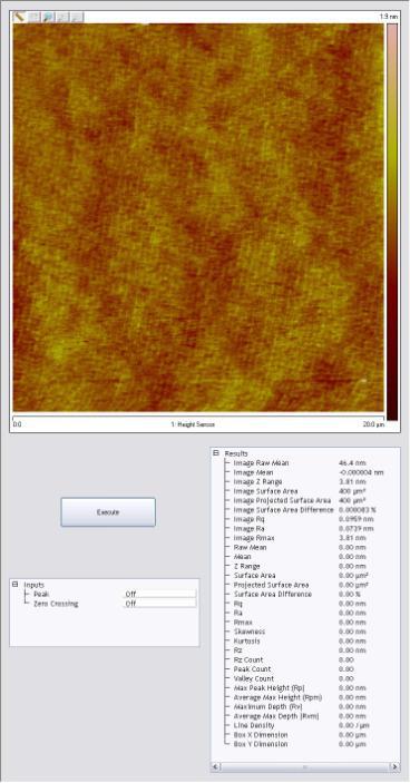
| Surface finish (Si-face): | Epi-ready (CMP) Rq ≤ 0.2 nm |
| Surface finish (C-face): | Optical Rq ≤ 3.0 nm |
| 
 |
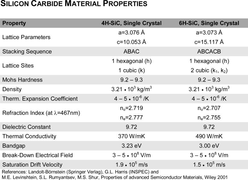
Silicon Carbide Material Properties
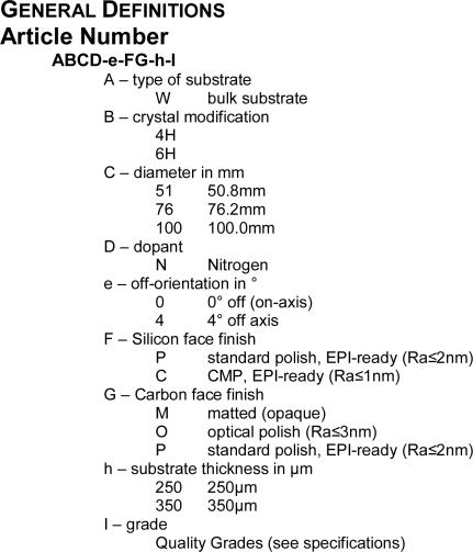
General Definitions Article Number
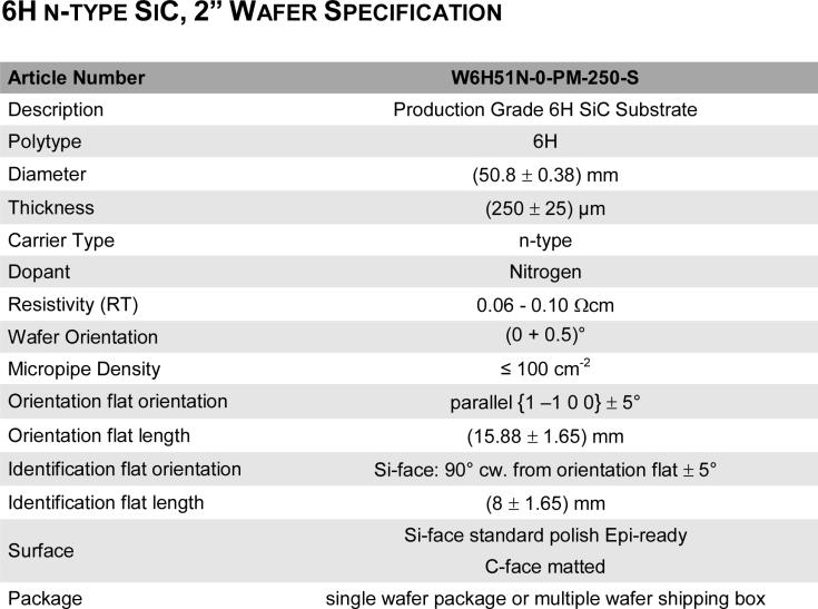
6H N_TYPE Sic,2" Wafer Specification
ATTENTION
Efforts products are designed exclusively for the use in electronic components.
Specifications are subject to change without notice. |
4H N_TYPE Sic,100MM Wafer Specific Ation
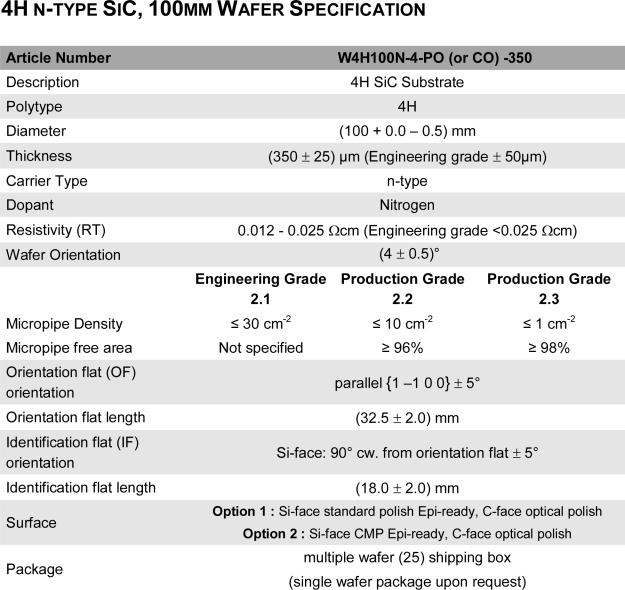
ATTENTION
Efforts products are designed exclusively for the use in electronic components.
Specifications are subject to change without notice. |
4H N_TYPE Sic,3",250μm Wafer Specification
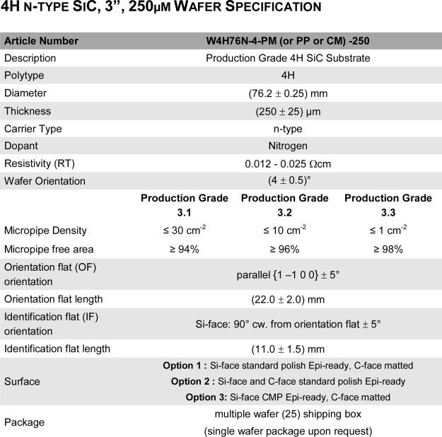
ATTENTION
Efforts products are designed exclusively for the use in electronic components.
Specifications are subject to change without notice. |
4H N_TYPE Sic,3",350μm Wafer Specification
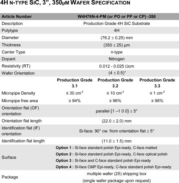
ATTENTION
Efforts products are designed exclusively for the use in electronic components.
Specifications are subject to change without notice.
|